- 您现在的位置:买卖IC网 > Sheet目录483 > NDD04N50Z-1G (ON Semiconductor)MOSFET N-CH 500V 3A IPAK
�� �
�
�NDD04N50Z�
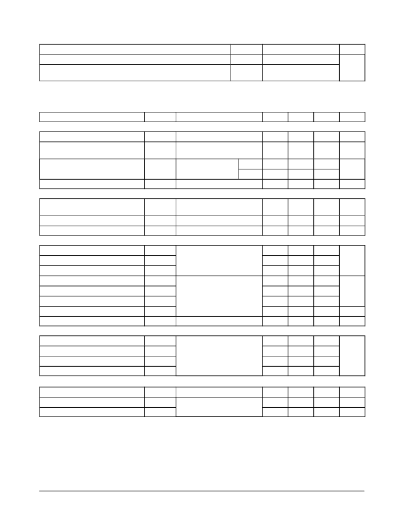
�THERMAL� RESISTANCE�
�Parameter�
�Symbol�
�Value�
�Unit�
�Junction� ?� to� ?� Case� (Drain)�
�Junction� ?� to� ?� Ambient� Steady� State�
�NDD04N50Z�
�(Note� 3)� NDD04N50Z�
�(Note� 2)� NDD04N50Z� ?� 1�
�R� q� JC�
�R� q� JA�
�2.0�
�40�
�80�
�°� C/W�
�2.� Insertion� mounted�
�3.� Surface� mounted� on� FR4� board� using� 1� ″� sq.� pad� size,� (Cu� area� =� 1.127� in� sq� [2� oz]� including� traces).�
�ELECTRICAL CHARACTERISTICS� (T� J� =� 25� °� C� unless� otherwise� noted)�
�Characteristic�
�Symbol�
�Test� Conditions�
�Min�
�Typ�
�Max�
�Unit�
�OFF� CHARACTERISTICS�
�Drain� ?� to� ?� Source� Breakdown� Voltage�
�Breakdown� Voltage� Temperature� Coeffi-�
�cient�
�BV� DSS�
�D� BV� DSS� /�
�D� T� J�
�V� GS� =� 0� V,� I� D� =� 1� mA�
�Reference� to� 25� °� C,�
�I� D� =� 1� mA�
�500�
�0.6�
�V�
�V/� °� C�
�Drain� ?� to� ?� Source� Leakage� Current�
�Gate� ?� to� ?� Source� Forward� Leakage�
�I� DSS�
�I� GSS�
�V� DS� =� 500� V,� V� GS� =� 0� V�
�V� GS� =� ±� 20� V�
�25� °� C�
�150� °� C�
�1.0�
�50�
�±� 10�
�m� A�
�m� A�
�ON� CHARACTERISTICS� (Note� 4)�
�Static� Drain� ?� to� ?� Source�
�On� ?� Resistance�
�Gate� Threshold� Voltage�
�Forward� Transconductance�
�R� DS(on)�
�V� GS(th)�
�g� FS�
�V� GS� =� 10� V,� I� D� =� 1.5� A�
�V� DS� =� V� GS� ,� I� D� =� 50� m� A�
�V� DS� =� 15� V,� I� D� =� 1.5� A�
�3.0�
�2.3�
�2.1�
�2.7�
�4.5�
�W�
�V�
�S�
�DYNAMIC� CHARACTERISTICS�
�Input� Capacitance� (Note� 5)�
�Output� Capacitance� (Note� 5)�
�Reverse� Transfer� Capacitance� (Note� 5)�
�Total� Gate� Charge� (Note� 5)�
�Gate� ?� to� ?� Source� Charge� (Note� 5)�
�Gate� ?� to� ?� Drain� (“Miller”)� Charge� (Note� 5)�
�C� iss�
�C� oss�
�C� rss�
�Q� g�
�Q� gs�
�Q� gd�
�V� DS� =� 25� V,� V� GS� =� 0� V,�
�f� =� 1.0� MHz�
�V� DD� =� 250� V,� I� D� =� 3.4� A,�
�V� GS� =� 10� V�
�246�
�33�
�7.0�
�6.0�
�1.3�
�3.5�
�308�
�43�
�9.0�
�12�
�2.6�
�6.1�
�370�
�53�
�11�
�18�
�4.0�
�7.0�
�pF�
�nC�
�Plateau� Voltage�
�V� GP�
�6.6�
�V�
�Gate� Resistance�
�R� g�
�1.8�
�5.4�
�16.2�
�W�
�RESISTIVE� SWITCHING� CHARACTERISTICS�
�Turn� ?� On� Delay� Time�
�t� d(on)�
�9.0�
�ns�
�Rise� Time�
�Turn� ?� Off� Delay� Time�
�Fall� Time�
�t� r�
�t� d(off)�
�t� f�
�V� DD� =� 250� V,� I� D� =� 3.4� A,�
�V� GS� =� 10� V,� R� G� =� 5� W�
�9.0�
�16�
�10�
�SOURCE� ?� DRAIN� DIODE� CHARACTERISTICS� (T� C� =� 25� °� C� unless� otherwise� noted)�
�Diode� Forward� Voltage�
�Reverse� Recovery� Time�
�Reverse� Recovery� Charge�
�V� SD�
�t� rr�
�Q� rr�
�I� S� =� 3.4� A,� V� GS� =� 0� V�
�V� GS� =� 0� V,� V� DD� =� 30� V�
�I� S� =� 3.4� A,� di/dt� =� 100� A/� m� s�
�240�
�0.9�
�1.6�
�V�
�ns�
�m� C�
�4.� Pulse� Width� ≤� 380� m� s,� Duty� Cycle� ≤� 2%.�
�5.� Guaranteed� by� design.�
�http://onsemi.com�
�2�
�发布紧急采购,3分钟左右您将得到回复。
相关PDF资料
NDD05N50ZT4G
MOSFET N-CH 500V 5A DPAK
NDF02N60ZH
MOSFET N CH 600V 2.4A TO220FP
NDF03N60ZH
MOSFET N CH 600V 4.8A TO220FP
NDF04N60ZH
MOSFET N CH 600V 4.8A TO220FP
NDF04N62ZG
MOSFET N-CH 620V 2OHM TO220FP
NDF05N50ZH
MOSFET N-CH 500V 4.4A TO-220FP
NDF06N60ZG
MOSFET N-CH 600V 7.1A TO-220FP
NDF06N60ZH
MOSFET N CH 600V 7.1A TO220FP
相关代理商/技术参数
NDD04N50ZT4G
功能描述:MOSFET 500V 3A HV MOSFET DPAK RoHS:否 制造商:STMicroelectronics 晶体管极性:N-Channel 汲极/源极击穿电压:650 V 闸/源击穿电压:25 V 漏极连续电流:130 A 电阻汲极/源极 RDS(导通):0.014 Ohms 配置:Single 最大工作温度: 安装风格:Through Hole 封装 / 箱体:Max247 封装:Tube
NDD04N60Z
制造商:ONSEMI 制造商全称:ON Semiconductor 功能描述:N-Channel Power MOSFET 1.8 , 600 Volts
NDD04N60Z-1G
功能描述:MOSFET NFET IPAK 600V 4A 1.8R RoHS:否 制造商:STMicroelectronics 晶体管极性:N-Channel 汲极/源极击穿电压:650 V 闸/源击穿电压:25 V 漏极连续电流:130 A 电阻汲极/源极 RDS(导通):0.014 Ohms 配置:Single 最大工作温度: 安装风格:Through Hole 封装 / 箱体:Max247 封装:Tube
NDD04N60ZG
制造商:ON Semiconductor 功能描述:NDD Series 600 V 1.8 Ohm 83 W Surface Mount N-Channel Power MOSFET - TO-252-3
NDD04N60ZT4G
功能描述:MOSFET NFET DPAK 600V 4A 1.8R RoHS:否 制造商:STMicroelectronics 晶体管极性:N-Channel 汲极/源极击穿电压:650 V 闸/源击穿电压:25 V 漏极连续电流:130 A 电阻汲极/源极 RDS(导通):0.014 Ohms 配置:Single 最大工作温度: 安装风格:Through Hole 封装 / 箱体:Max247 封装:Tube
NDD04N62Z
制造商:ONSEMI 制造商全称:ON Semiconductor 功能描述:N-Channel Power MOSFET 620 V, 1.8
NDD04N62Z-1G
制造商:ONSEMI 制造商全称:ON Semiconductor 功能描述:N-Channel Power MOSFET 620 V, 1.8
NDD04N62ZT4G
制造商:ONSEMI 制造商全称:ON Semiconductor 功能描述:N-Channel Power MOSFET 620 V, 1.8